The arrays are assembled onto PCBs containing the MT guide pins. The PCBs are connected to a TX PCB for the VCSEL array and an RX PCB for the PIN array (see PK's talk for more info) . The TX PCB also contains the BPM-12 PCB and multi-DACs. The RX PCB also contains the DRX-12 PCB. These TX and RX PCBs plug into the BOC PCB.
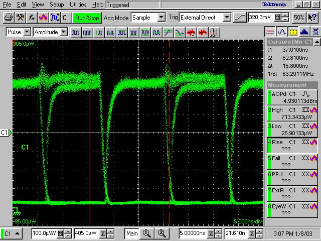
High power versions of the Oxide implant VCSEL arrays have been obtained from Truelight. The first TX plug-in with these high power versions of the VCSELs was made by Minglee. All 12 channels are functional. The power at digital "1" are in the range 1.2 mW to 1.4 mW for a DAC current in the range 11 to 12 mA. The rise and fall times (20%-80%) are about 1 nS. A scope picture of the optical output of one channel of this array being driven by the BPM-12 chip on a TX PCB is available here .
12 way arrays of silicon PIN diodes are used.
Minglee's scope photos of the response of one channel of a PIN array to optical signals at different PIN bias voltages are available here. Maurice has compile a summary plot showing the baseline shift as a function of bias voltage see his pdf file here
Maurice and Tony also studied the response of the PIN array at different bias voltages. The PIN was mounted on an RX plug-in with a DRX-12 chip. The results were similar to Minglee's.
From this scan the rise and fall times decrease with increasing PIN bias voltage and then reach a plateau at a PIN bias voltage of about 6V. There is also a slow component to the fall time. The amplitude of this component was estimated by measuring the baseline 20 ns after the signal turned off (where the signal was a long burst of "1"s). Further measurements and analysis from Maurice are available here.
The PIN response was measured at higher currents by using VCSELs in a pre-series harness. The results are available here.
The performance of the PIN array/DRX-12 system was studies on an RX plug-in PCB mounted on a modified OptIF-B card. This allowed us to vary the bias voltage on the PIN in the range 0 to 15V. The results of the first set of measurements are available as a note here.